New Applied Materials R&D Center to Help Customers Overcome Moore’s Law Challenges
SANTA CLARA, Calif.,
|
|||||
The primary goal of the META Center is to speed customer availability of new chipmaking materials and process technologies that enable breakthroughs in semiconductor performance, power and cost. The new center will complement and extend the capabilities of Applied’s Maydan Technology Center in
The META Center will be a hub for innovation, delivering on a call to action by Applied CEO Gary Dickerson for increased collaboration and speed across the technology ecosystem.
“Realizing the full potential of Artificial Intelligence and Big Data will require significant improvements in performance, power consumption and cost both at the edge and in the cloud,” said Gary Dickerson, president and CEO of Applied Materials. “The industry needs new computing architectures and chips enabled by innovative materials and scaling approaches. The META Center creates a new platform for working with customers to accelerate innovation from materials to systems.”
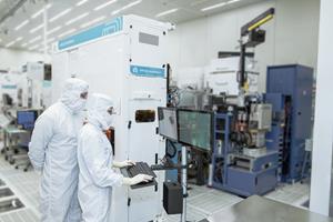
Scheduled to open in 2019, the META Center will be a first-of-its kind facility, spanning 24,000 square feet of cleanroom. It will be furnished with a broad suite of Applied’s most advanced process systems along with complementary technologies needed for new chip materials and structures to be piloted for high-volume production at customer sites.
To be located at the State University of New York Polytechnic Institute (SUNY Poly) campus in Albany, New York, the META Center will be created under agreements to be entered into with New York State, The Research Foundation for
“SUNY Poly provides an ideal combination of infrastructure, capabilities and talent in a thriving academic and entrepreneurial setting with deep roots in the semiconductor industry,” said Steve Ghanayem, senior vice president of New Markets and Alliances at Applied Materials. “The technology ecosystem will benefit from the acceleration of materials innovation through collaboration at the META Center.”
Industry Comments
According to Samsung R&D, “We value our collaboration with Applied Materials on process development. The industry needs new innovations beyond traditional device scaling including the exploration of new materials. We are very pleased to see Applied Materials’ effort to expand its advanced R&D capabilities to provide added resources to customers and accelerate chip development.”
“TSMC welcomes closer collaboration with critical suppliers like Applied Materials in both equipment and materials,” said J.K. Lin, TSMC’s Vice President of Information Technology and Risk Management & Materials Management. “Working together to accelerate the industry’s innovation and address high-growth opportunities is very much in the spirit of TSMC’s
“IBM and Applied Materials have a long history of collaboration in materials engineering to advance semiconductor industry breakthroughs,” said Dr. Mukesh V. Khare,
“As complexity increases and costs rise, traditional device scaling is slowing for the latest technology nodes,” said Tom Caulfield, CEO GLOBALFOUNDRIES. “It's great to see Applied Materials investing in a broad range of advanced R&D capabilities to bring new and new combinations of materials into chip manufacturing, and I look forward to our continued collaborative efforts as we develop more differentiated solutions for our clients.”
“Delivering the improvements in performance and efficiency that allow Arm partners to continue to advance compute will mean overcoming the challenges presented by scaling transistors and interconnect in the deep nanometer process nodes,” said Greg Yeric, fellow, Arm. “There are many novel ideas being explored in this area, but the timeline from concept to production needs to be accelerated, and the expansion of Applied Materials’ R&D capabilities will help enable this research to advance at a faster pace.”
“Applied Materials is the world leader in semiconductor process and tools,” said Kurt Busch, CEO of
Forward-Looking Statements
This press release contains forward-looking statements, including but not limited to those regarding plans and expectations for the proposed research and development facility, industry outlook and technology requirements, the development of new materials and technologies, and other statements that are not historical facts. These statements and their underlying assumptions are subject to risks and uncertainties and are not guarantees of future performance. Factors that could cause actual results to differ materially from those expressed or implied by such statements include, without limitation: the ability of the parties to consummate the agreements under which the facility will be created; the ability to secure regulatory and other approvals in a timely manner or at all; the demand for semiconductors and customers’ technology requirements; our ability to develop new and innovative technologies; our ability to obtain and protect intellectual property rights in key technologies; our ability to achieve the operational objectives of the proposed facility; and other risks and uncertainties described in our SEC filings, including our most recent Forms 10-Q and 8-K. All forward-looking statements are based on management’s current estimates, projections and assumptions, and we assume no obligation to update them.
About Applied Materials
Applied Materials, Inc. (Nasdaq: AMAT) is the leader in materials engineering solutions used to produce virtually every new chip and advanced display in the world. Our expertise in modifying materials at atomic levels and on an industrial scale enables customers to transform possibilities into reality. At Applied Materials, our innovations make possible the technology shaping the future. Learn more at www.appliedmaterials.com.
Contact:
Ricky Gradwohl (editorial/media) 408.235.4676
Michael Sullivan (financial community) 408.986.7977
A photo accompanying this announcement is available at http://www.globenewswire.com/NewsRoom/AttachmentNg/2d32082b-f76a-4bcf-a5d4-6f12aac17ee9
This photo is also available at Newscom, www.newscom.com, and via AP PhotoExpress.

