Applied Materials Unveils eBeam Metrology System that Enables a New Playbook for Patterning Advanced Logic and Memory Chips
- Today’s leading-edge chip designs require a new class of metrology that goes beyond optical target-based approximation, statistical sampling and single-layer control
- PROVision® 3E system combines nanometer resolution, high speed and through-layer imaging to give engineers the millions of datapoints they need to correctly pattern the most advanced chip designs
- 30 systems already installed at the world’s leading foundry-logic, DRAM and NAND customers
Advanced chips are built one layer at a time, and each of billions of individual features must be perfectly patterned and aligned to create working transistors and interconnects with optimal electrical characteristics. As the industry increasingly moves from simple 2D designs to more aggressive multipatterning and 3D designs, a commensurate breakthrough in metrology is needed to perfect each critical layer and enable the best performance, power, area-cost and time to market (PPACt™).
Traditional Patterning Control Playbook
Traditionally, patterning control has been achieved using optical overlay tools that help align die patterns with “proxy targets” which are guide marks printed into the spaces between die that are removed from the wafer during die singulation. Proxy target approximation has been complemented with statistical sampling of a small number of die patterns from across the wafer.
However, after successive generations of feature shrinking, broader adoption of multipatterning, and the introduction of 3D designs that cause interlayer distortions, the traditional approach is leading to measurement deficiencies – or “blind spots” – that are making it more difficult for engineers to correlate intended patterns with on-die results.
New Patterning Control Playbook
With the arrival of new eBeam system technology that can directly measure semiconductor device structures across the wafer and through layers at high speed, customers are moving to a new patterning control playbook based on big data. Applied’s latest eBeam metrology innovation – the PROVision® 3E system – is especially designed for this new playbook.
“As the leader in eBeam technology,
PROVision 3E System
The PROVision 3E system includes technical features that enable patterning control of today’s most advanced designs, including 3nm foundry-logic chips, gate-all-around transistors and next-generation DRAM and 3D NAND.
- Resolution: Applied’s industry-leading eBeam column technology provides the highest electron density available, enabling detailed imaging at 1nm resolution.
- Accuracy: Decades of CD SEM system and algorithm expertise deliver accurate and precise measurements of critical features.
- Speed: 10 million accurate, actionable measurements per hour.
- Multi-Layer: Applied’s unique Elluminator® technology captures 95 percent of back-scattered electrons to quickly measure critical dimensions and edge placement at multiple levels simultaneously.
- Range: A broad range of eBeam energies. High-energy modes enable rapid measurement, hundreds of nanometers deep. Low-energy modes enable damage-free measurement of fragile materials and structures including EUV photoresist.
Together, these features enable customers to move from the old patterning control playbook – composed of optical proxy target approximation, limited statistical sampling and single-layer control – to a new playbook based on massive on-device, across-wafer and through-layer metrology and control.
Process Recipe Optimization
The PROVision 3E system is also a key component of Applied’s AIx™ (Actionable Insight Accelerator) platform which combines process technology, sensors, metrology and data analytics to accelerate every stage of process technology development – from R&D to ramp and high-volume manufacturing. AIx platform analytics correlate process variables with the on-wafer measurements captured by the PROVision 3E system, helping engineers speed process development by 2X and widen process windows by 30 percent.
Availability
The PROVision 3E system is now being used by leading foundry-logic, DRAM and NAND customers worldwide. Additional information about patterning control, the PROVision 3E system and process recipe optimization will be discussed at Applied’s 2021
About
Contact:
A photo accompanying this announcement is available at https://www.globenewswire.com/NewsRoom/AttachmentNg/543b33ab-e1d1-4be8-9179-5fd95aa93a01
These photos are also available at Newscom, www.newscom.com, and via AP PhotoExpress.

![]()
Applied Materials’ PROVision® 3E eBeam metrology system image
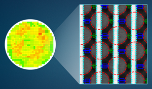
Applied Materials’ new PROVision® 3E eBeam metrology system enables a new playbook for patterning control by combining nanometer resolution, high speed and through-layer imaging to give engineers the millions of datapoints they need to correctly pattern the most advanced chip designs.
Source: Applied Materials, Inc.